
When Matthew Marinella left a research position at Sandia National Laboratories to become an associate professor of electrical engineering at Arizona State University, he didn’t let go of his ties to Sandia.
Since joining the faculty of ASU’s Ira A. Fulton Schools of Engineering, Marinella has continued to collaborate with Sandia on her research. For example, he is the principal investigator of a project to increase computing performance through greater power efficiency for radiation-hardened, or ‘rad-hard’, electronics in the Science Research Series Great Sandia Challenge. The work at ASU builds on previous electronics research conducted by Marinella at Sandia.
Radiation hardening is a process that increases the durability of electronics used in high radiation environments like outer space. This can allow crucial computer components, such as those in a spacecraft, to function where ordinary electronics would fail under radiation exposure.
Sandia’s Grand Challenge projects are considered high-risk, high-reward and are funded for three years.
Source: Adobe Images
“I started at ASU in January 2022, coming from Sandia where we had been working on a really big project like this for several years,” says Marinella. “It was eventually funded, so of course we’re hoping this work will lead to bigger projects.”
Collaborators from the University of California at Berkeley, the University of Texas at Austin and the University of Michigan are also involved in this Grand Challenge research. The project’s senior management sponsor and strategic research client at Sandia, Rick McCormick, says the researchers from these institutions were recruited for their expertise in emerging analog computing devices, which are a key part of the project.
Used in radiation rich environments
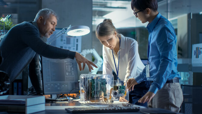
To increase the computational efficiency of radiation-hardened electronics beyond conventional capabilities, the research team is developing new analog devices that use resistive random-access memory, or ReRAM, and electrochemical random-access memory, or ECRAM. These analog devices will be combined in arrays laid on top of complementary metal oxide semiconductors, or CMOS, computer chips made by Taiwan Semiconductor Manufacturing Co.
Once developed, these devices would then be used in radiation-rich environments, both in space and on Earth.
“If you’ve seen Chernobyl or somewhere like that, you have robots trying to get to a place where you don’t want to put people,” Marinella says of the devices’ terrestrial uses.
Satellite cameras are another example of what increased processing efficiency could do. The capabilities of satellites are limited by parameters such as their size, weight and battery power. Making on-board computing more efficient, as with the technology Marinella’s team is developing, would free up energy for other tasks, including increasing the resolution of satellite photos.
Efficiency-enhancing memory chips
Marinella says the Department of Defense is interested in radiation-hardened computer technology, including for uses such as image processing with edge computing. In edge computing, data is processed in a computer system soon after it is collected, reducing the number of large raw data files to transfer and speeding up file exchange.
Although these chips are intended for use in radiation-resistant applications for now, Marinella sees efficiency-enhancing memory chip arrays, combined with traditional semiconductors, eventually becoming ubiquitous in consumer electronics.
“It would be the chip in your cell phone, in your self-driving vehicles, and in your cloud computing systems,” he says.
Transfer data between separate elements
According to Sapan Agarwal, principal investigator on the Sandia side of this Grand Challenge project, integrating memory devices with traditional chips will push the boundaries beyond what is possible with traditional chips alone. The processing efficiency of conventional CMOS chips is limited by the size and voltage of their transistors.
Agarwal says one of the biggest factors slowing down computing with conventional chips is the need to transfer data between separate elements for memory storage and processing. Integrating the team’s new ReRAM and ECRAM devices with CMOS chips will allow memory to be processed and stored in one place. According to Agarwal, this will result in compute performance per watt 100 times greater than is currently possible.
Finned field effect transistors
McCormick notes that the team will be experimenting with different analog computing devices, which will help them determine which is best for their applications. Marinella is also working on a separate project with Hugues Barnabe, a professor of electrical engineering at ASU, to understand the effects of radiation on transistors known as finned field-effect transistors, or FinFETs, which are more efficient than older standard node transistors. While this project is also a collaboration with and funded by Sandia, it is separate from Marinella’s work in the Grand Challenge program focused on integrating CMOS chips with analog device arrays.
Although the Grand Challenge project combining CMOS chips with analog devices will not use FinFETs for research, Marinella’s future goal is to use FinFETs as transistors for CMOS chips and integrated analog arrays if FinFETs are found to tolerate extreme radiation fairly well. environments. The more efficient combination would release even more radiation-enhanced computing power, making the system even more efficient than the current Grand Challenge CMOS and analog memory integration project.
Contribute to the development of key enabling technologies
McCormick says having Marinella work at ASU, after her excellent record of innovation and training postdoctoral researchers at Sandia, puts the two institutions in an excellent position for research collaboration opportunities.
“Matt has already connected us with other high-impact faculty at ASU and has maintained strong collaborations with Sandia,” he says. “We look forward to continuing to work with him and having him train the next generation of Sandia researchers.”
Agarwal agrees that the partnership with ASU is a great opportunity to expand Sandia’s research capabilities.
“The ASU team is at the heart of our broader research efforts, helping to develop key technologies and partnering with us on our broader emerging microelectronics strategy,” he said. . “At ASU, Matt continues to be an essential contributor.”